


HOME→Automatic silicon wafer grinder Automatic silicon wafer grinder Automatic silicon wafer grinder
MTW European Type Trapezium Mill
Input size:30-50mm
Capacity: 3-50t/h
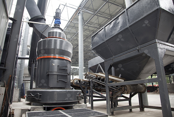
LM Vertical Roller Mill
Input size:38-65mm
Capacity: 13-70t/h
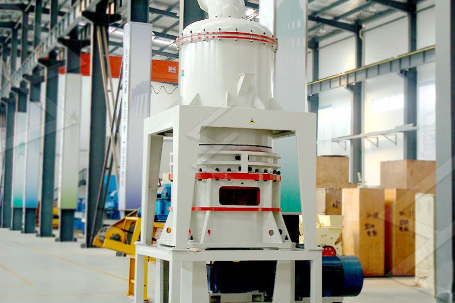
Raymond Mill
Input size:20-30mm
Capacity: 0.8-9.5t/h
Sand powder vertical mill
Input size:30-55mm
Capacity: 30-900t/h
LUM series superfine vertical roller grinding mill
Input size:10-20mm
Capacity: 5-18t/h
MW Micro Powder Mill
Input size:≤20mm
Capacity: 0.5-12t/h
LM Vertical Slag Mill
Input size:38-65mm
Capacity: 7-100t/h

LM Vertical Coal Mill
Input size:≤50mm
Capacity: 5-100t/h
TGM Trapezium Mill
Input size:25-40mm
Capacity: 3-36t/h
MB5X Pendulum Roller Grinding Mill
Input size:25-55mm
Capacity: 4-100t/h
Straight-Through Centrifugal Mill
Input size:30-40mm
Capacity: 15-45t/h
Automatic silicon wafer grinder Automatic silicon wafer grinder Automatic silicon wafer grinder
Manufacturing Equipment for Silicon Wafer SpringerLink
2023年11月28日 This chapter introduces 15 kinds of main silicon wafer manufacturing equipment, including Single Crystal Growth Furnace, Float Zone Crystal Growth Furnace, 6 天之前 The capability to quickly and efficiently produce quality wafer surfaces in pilot line and R D applications is key in today’s rapidly changing semiconductor environment The engineers at Engis have developed a grind Semiconductor Grinding, Lapping, Polishing AsiaPacific, particularly China, leads the global Automatic Silicon Wafer Grinders market, with robust domestic demand, supportive policies, and a strong manufacturing base Key Features: Global Automatic Silicon Wafer Grinders Market 2024 by 2022年12月15日 For grinding wafers smaller than 8inches, DISCO has been providing the fully automatic grinder DFG8540, which has been shipped to many device manufacturers and electric component manufacturers as a standard Disco develops fully automatic grinder for 100
.jpg)
Surface Grinding in Silicon Wafer Manufacturing
2003年6月5日 surface grinding possesses the great potential of producing silicon wafers with lower cost and better quality comparing with its counterparts (lapping for wire sawn wafers Picture: DISCO’s new DFG8640 wafer grinding system Waferlevel thinning and grinding targeting lowheight semiconductor memory and logic memory are essential for high functionality and high space efficiency of final products Disco launches highprecision fully automatic 8 2008年10月1日 This review paper discusses historical perspectives on grinding of silicon wafers, impacts of wafer size progression on applications of grinding in silicon wafer manufacturing, Grinding of silicon wafers: A review from historical perspectives2006年5月21日 In this investigation, a threevariable twolevel full factorial design is employed to reveal the main effects as well as the interaction effects of three process parameters (wheel Fine grinding of silicon wafers: designed experiments
Experimental Investigations of Silicon Wafer Grinding
2006年9月17日 To manufacture highquality silicon wafers, a series of processes are needed ・The process from back grinding to wafer mounting continuously by fully automatic system, which enable to grind till 25um thickness ・With 2 head polishing stage, throughput is almost double compared with 1 polish head system ・Built in edge trimming system is available as an option for thin wafer processWafer Backside Grinding 株式会社岡本工作機械製作所 バック 2020年8月18日 Silicon wafers are the most widely used substrate material in integrated circuit manufacturing [1,2,3]Back grinding of wafer with outer rim (BGWOR) is a new method for carrierless thinning of silicon wafers, and its working principle is shown in Fig 1Different from conventional back grinding, the BGWOR process only grinds the inner area of the silicon wafer Study into grinding force in back grinding of wafer with outer Achieving the correct wafer thickness before assembly is a key factor in semiconductor manufacturing Wafer back grinding (or wafer thinning) is a semiconductor manufacturing process designed to control the wafer thickness, essential to produce ultrathin wafers used to create stacked and highdensity packaging in compact electronic devicesBack Grinding: Wafer Thinning Marposs
Fine grinding of silicon wafers: designed experiments
2006年5月21日 The grinder records the grinding force automatically The grinding force measured is the interaction force between the grinding wheel and the wafer in the direction parallel to the spindle axis It is also the direction perpendicular to the wafer surface The maximum force during the entire grinding cycle is used for analysis The4 天之前 We offer systems for highprecision wafer edge profiling directly after the wafers have been sawn out of the silicon single crystal (ingot) The modular system of the ACCRETECH Wafer Edge Grinder can be configured for wafer sizes from 212″ and for diverse materials (Si, GaAs, sapphire Si, SiC)Your partner for precise wafer edge grinding ACCRETECH (Europe)2023年11月28日 It has the advantages of high processing efficiency, good wafer surface flatness, low cost, little surface damage, etc After the singlesided surface grinding process, the Si wafer surface has many obvious grinding marks, which will affect the surface nanotopography of Si polished waferSilicon Wafer Processing SpringerLink6 天之前 UV curable or standard adhesive backgrinding tape is temporarily applied to protect your silicon wafers from damage during wafer grinding Specifications Our capabilities include: Thin wafers from 4” to 8” diameter; Backgrinding to target thickness of 0025mm (0001”) Single die, partial wafer, or bumped wafer backgrindingSilicon Wafer Backgrinding Wafer Thinning Services
Silicon Wafer Automatic Batchtype Cleaning Device
2023年9月15日 Device Introduction Silicon Wafer Batchtype Automatic Cleaning Device Introduction of silicon wafer cleaning device 1 Postlapping cleaning equipment: Lapping abrasive grain removal (alkali + interfacebased cleaning mainly) 2 Alkali etching and cleaning device: Cleaning equipment designed to remove process distortions after grinding 32006年9月17日 Experimental Investigations of Silicon Wafer Grinding JH Liu 1,a, ZJ Pei 1,b and Graham R Fisher 2,c 1Department of Industrial and Manufacturing Systems Engineering, Kansas State University, Manhattan, KS 66506, USA 2MEMC Electronic Materials, Inc, 501 Pearl Drive, St Peters, MO 63376, USA ajinghua@ksu, b zpei@ksu, cGFisher@memc Experimental Investigations of Silicon Wafer Grinding2 天之前 Equipped with automatic slurry dosing devices, it makes the most of the slurry, reduces slurry waste and saves consumables cost while meeting environmental requirement 7 The use of Japanese "NSK" shafting, Japanese "SMC" pneumatic components, maintenancefree power plant of Japanese "Sumitomo" and Swiss "ABB" electrical components ensures Automatic Silicon Wafer Lapping and Polishing MachineSilicon Wafer Silicon wafers are the most common substrate used in semiconductor manufacturing Our precise back grinding techniques ensure uniform thickness and exceptional flatness for optimal device performance Silicon Wafer Back Grinding/Wafer Thinning
.jpg)
Grinding of silicon wafers: a review from historical
2009年11月25日 discusses historical perspectives on grinding of silicon wafers, impacts of wafer size progression on applications of grinding in silicon wafer manufacturing, and interrelationships between grinding and two other silicon machining processes (slicing and polishing) It is intended to help ∗ Corresponding author Tel: +1 785 532 3436; fax 2024年1月25日 This study aims to analyze the nanogrinding behavior of silicon wafer workpieces with nanoscale roughness by molecular dynamics simulations The nanogrinding process of silicon wafer workpieces with varying rootmeansquare roughness under different grinding depths is simulated, considering synchronous rotation and translation of the diamond Molecular Dynamics Study of NanoGrinding Behavior for Silicon Wafer 2024年11月24日 Application: back thinning, front grinding and fine grinding of discrete devices, integrated circuit substrate silicon wafers, sapphire epitaxial wafers, silicon Back Grinding Wheel for Surface Grinding Various Silicon Wafer2023年1月2日 JTEKT recently demonstrated a new doubledisc horizontal grinder that simultaneously grinds both sides of silicon wafers to +/ 1 micron from assliced condition The DXSG320 performance represents a massive improvement in accuracy and productivity over the singlespindle vertical grinders common in the chip industry today which grind to 34 microns, JTEKT Introduces new Highproductivity Silicon Wafer Disc Grinder
Automatic Wafer Grinders Market Size 2024 Analysis By
2024年7月22日 Automatic wafer grinders play a crucial role in the semiconductor manufacturing process, enabling precise grinding of silicon wafers to achieve the required thickness and surface smoothness2012年9月1日 This study presents design of an ultraprecision wafer grinder which incorporates stateoftheart automatic supervision and control system The wafer grinder is characterized by wafer surface shape control, grinding forces and wafer thickness monitoring systems The design provides a totally integrated solution to the ultraprecision grinder that is capable of grinding Development of UltraPrecision Grinder for 300mm Wafers2024年11月11日 The edge grinders “WGM series” process edge grinding of various kind of materials such as Silicon, sapphire and SiCAs a solution for that, Our WGM series are highly rated among manufactures of silicon, compound materials and other wafer shaped materials Wafer edge grinding machine also draws the attention as a solution for the yield lossEdge Grinding Machines Semiconductor Manufacturing 2024年7月23日 grinder During grinding, the silicon wafer was held on a porous ceramic vacuum chuck, the grinding wheel and the wafer rotate about their own axis simultaneously, and theEdge chipping of silicon wafers in rotating grinding
.jpg)
Effects of taping on grinding quality of silicon wafers in backgrinding
2021年4月19日 A predictive model of grinding force in silicon wafer selfrotating grinding International Journal of Machine Tools and Manufacture, 2016, 109: 74–86 Article Google Scholar Lin B, Zhou P, Wang Z, et al Analytical elasticplastic cutting model for predicting grain depthofcut in ultrafine grinding of silicon wafer2008年10月1日 The grinding process involves a complicated superposition process of surface scratches, but its atomic mechanism is still unclear In this work, the molecular dynamics (MD) simulations of silicon Grinding of silicon wafers: A review from historical perspectives2015年12月10日 If the bonding adhesive has a different thickness variation on each wafer, “RAuto TTV” is more effective, where “R” represents regrinding “Auto TTV” returns a TTV adjustment value for use with the next wafer On the Wafer Handling and Thinning Processes2024年4月26日 Automatic Silicon Wafer Grinders Market Competitive Analysis Competitive analysis indicates that the market is highly competitive with a few key players dominating the industry The market is Automatic Silicon Wafer Grinders Market Size, Share
.jpg)
DAG810 – AUTOMATIC SURFACE GRINDER ‒ Center of
The DAG810 is a compact, automatic grinder for silicon, III/V materials (GaN, GaAs, InP) and various glass types (pure amorphous SiO2, float glass, pyrex) It is used to thin down single wafers, stacked wafers or chips of any shapes and dimensions (from a few mm2 to full 8″ wafer) Figure 2: Silicon test wafer before grinding (left 2024年1月15日 0; At WaferPro, we provide specialized fabrication and processing services for both glass and silicon wafer substratesBut understanding the nuanced differences between these two ubiquitous materials is key to selecting the optimal option for your semiconductor, microelectronic, photonic, or biotech applicationGlass Wafer vs Silicon Wafer: An InDepth Comparison2023年8月3日 Silicon already reacts with oxygen at room temperature to form SiO 2, the silicon dioxideSiO 2 is a highquality, mechanically and electrically stable insulator that can be selectively and reproducibly applied to the semiconductor employing temperature treatments This “speciesspecific” oxide is particularly advantageous for electrical insulation and local masking Silicon Wafer Production SpringerLink2006年5月21日 such issue is the grinding marks left on the wafer surface after fi ne grinding 15 Grinding marks Fig 3 shows pictures of two silicon wafers after fi ne grinding and polishing Wafer B is good since no patterns are visible, but wafer A is not acceptable due to visible grinding marks One approach to correct waferFine grinding of silicon wafers: a mathematical model for
Noncontact grinding/thinning of silicon carbide wafer by
2022年3月1日 The stateoftheart wafer grinding technology aims to obtain low damage and highquality surface at high efficiency so that the wafer manufacturing process can be shifted from grinding to CMP directly Thinning of a twoinch silicon carbide wafer by plasma chemical vaporization machining ssing a slit electrode Mater Sci Forum, 778–780 2024年8月13日 🌐 Automatic Silicon Wafer Grinders Market Research Report [20242031]: Size, Analysis, and Outlook Insights 🌐 Exciting opportunities are on the horizon for businesses and investors with the Automatic Silicon Wafer Grinders Market Size LinkedInThe Company has leveraged its significant intellectual property portfolio to develop the new flagship 6EZ Silicon Carbide Polisher, which, alongside the 7AFHMG Silicon Carbide Grinder, provides Revasum’s customers with an optimized, fully automated singlewafer grind and polish toolset The solution is configurable for SiC wafers 200mm and Revasum Semiconductor Grinding Technology・The process from back grinding to wafer mounting continuously by fully automatic system, which enable to grind till 25um thickness ・With 2 head polishing stage, throughput is almost double compared with 1 polish head system ・Built in edge trimming system is available as an option for thin wafer processWafer Backside Grinding 株式会社岡本工作機械製作所 バック
.jpg)
Study into grinding force in back grinding of wafer with outer
2020年8月18日 Silicon wafers are the most widely used substrate material in integrated circuit manufacturing [1,2,3]Back grinding of wafer with outer rim (BGWOR) is a new method for carrierless thinning of silicon wafers, and its working principle is shown in Fig 1Different from conventional back grinding, the BGWOR process only grinds the inner area of the silicon wafer Achieving the correct wafer thickness before assembly is a key factor in semiconductor manufacturing Wafer back grinding (or wafer thinning) is a semiconductor manufacturing process designed to control the wafer thickness, essential to produce ultrathin wafers used to create stacked and highdensity packaging in compact electronic devicesBack Grinding: Wafer Thinning Marposs2006年5月21日 The grinder records the grinding force automatically The grinding force measured is the interaction force between the grinding wheel and the wafer in the direction parallel to the spindle axis It is also the direction perpendicular to the wafer surface The maximum force during the entire grinding cycle is used for analysis TheFine grinding of silicon wafers: designed experiments4 天之前 We offer systems for highprecision wafer edge profiling directly after the wafers have been sawn out of the silicon single crystal (ingot) The modular system of the ACCRETECH Wafer Edge Grinder can be configured for wafer sizes from 212″ and for diverse materials (Si, GaAs, sapphire Si, SiC)Your partner for precise wafer edge grinding ACCRETECH (Europe)
.jpg)
Silicon Wafer Processing SpringerLink
2023年11月28日 It has the advantages of high processing efficiency, good wafer surface flatness, low cost, little surface damage, etc After the singlesided surface grinding process, the Si wafer surface has many obvious grinding marks, which will affect the surface nanotopography of Si polished wafer6 天之前 UV curable or standard adhesive backgrinding tape is temporarily applied to protect your silicon wafers from damage during wafer grinding Specifications Our capabilities include: Thin wafers from 4” to 8” diameter; Backgrinding to target thickness of 0025mm (0001”) Single die, partial wafer, or bumped wafer backgrindingSilicon Wafer Backgrinding Wafer Thinning Services2023年9月15日 Device Introduction Silicon Wafer Batchtype Automatic Cleaning Device Introduction of silicon wafer cleaning device 1 Postlapping cleaning equipment: Lapping abrasive grain removal (alkali + interfacebased cleaning mainly) 2 Alkali etching and cleaning device: Cleaning equipment designed to remove process distortions after grinding 3Silicon Wafer Automatic Batchtype Cleaning Device2006年9月17日 Experimental Investigations of Silicon Wafer Grinding JH Liu 1,a, ZJ Pei 1,b and Graham R Fisher 2,c 1Department of Industrial and Manufacturing Systems Engineering, Kansas State University, Manhattan, KS 66506, USA 2MEMC Electronic Materials, Inc, 501 Pearl Drive, St Peters, MO 63376, USA ajinghua@ksu, b zpei@ksu, cGFisher@memc Experimental Investigations of Silicon Wafer Grinding
Automatic Silicon Wafer Lapping and Polishing Machine
2 天之前 Equipped with automatic slurry dosing devices, it makes the most of the slurry, reduces slurry waste and saves consumables cost while meeting environmental requirement 7 The use of Japanese "NSK" shafting, Japanese "SMC" pneumatic components, maintenancefree power plant of Japanese "Sumitomo" and Swiss "ABB" electrical components ensures