


MTW European Type Trapezium Mill
Input size:30-50mm
Capacity: 3-50t/h
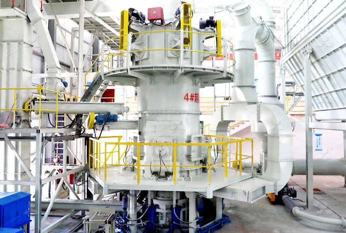
LM Vertical Roller Mill
Input size:38-65mm
Capacity: 13-70t/h
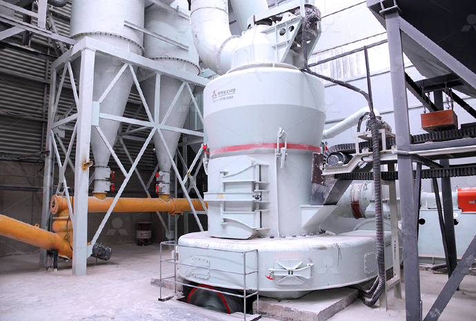
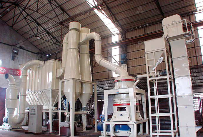
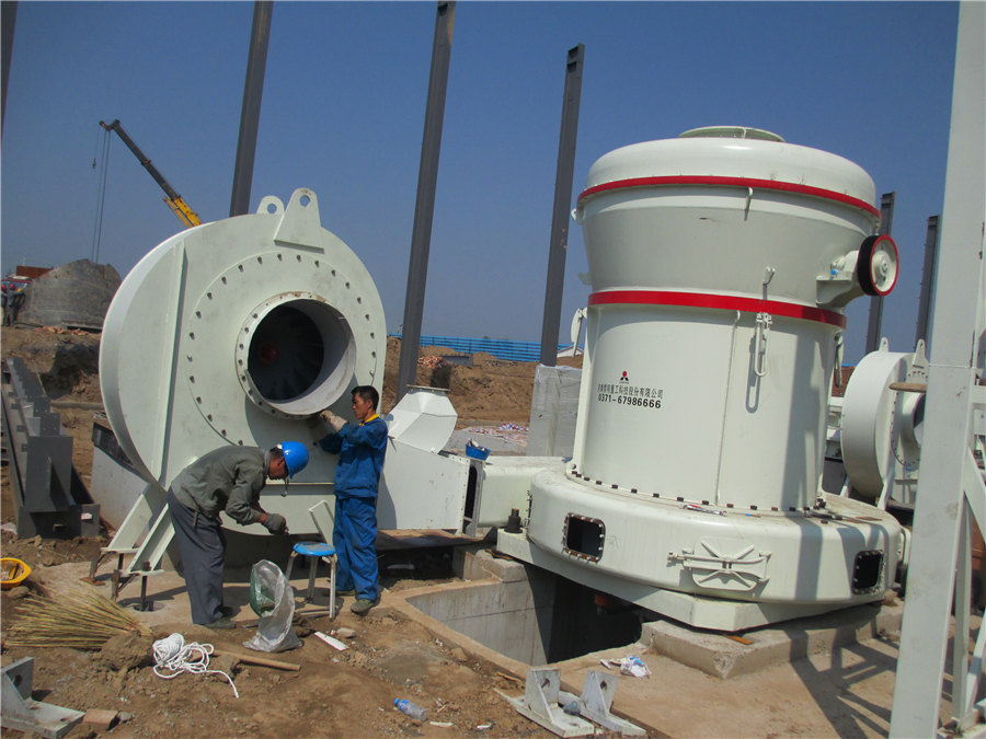
Raymond Mill
Input size:20-30mm
Capacity: 0.8-9.5t/h
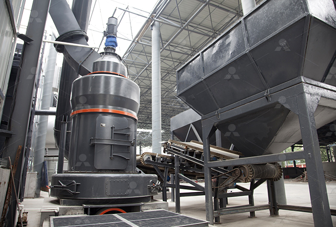
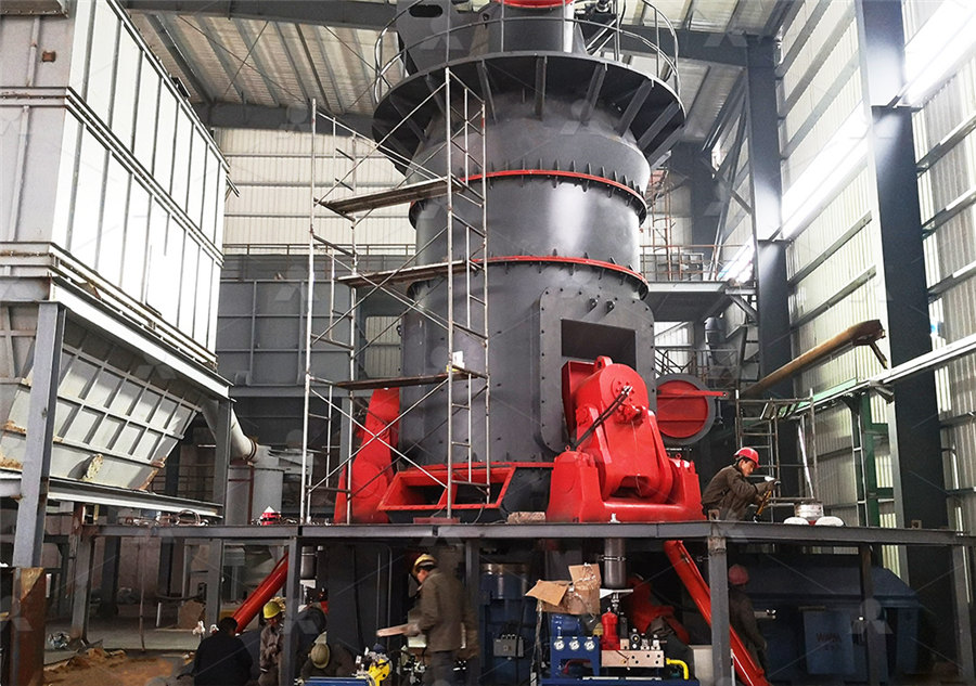
Sand powder vertical mill
Input size:30-55mm
Capacity: 30-900t/h
LUM series superfine vertical roller grinding mill
Input size:10-20mm
Capacity: 5-18t/h
MW Micro Powder Mill
Input size:≤20mm
Capacity: 0.5-12t/h
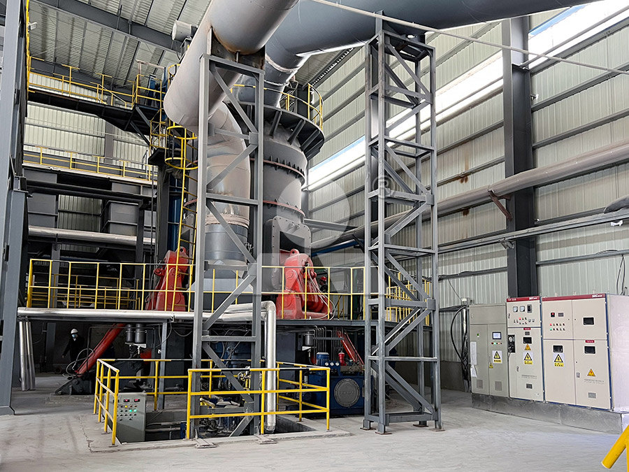
LM Vertical Slag Mill
Input size:38-65mm
Capacity: 7-100t/h

LM Vertical Coal Mill
Input size:≤50mm
Capacity: 5-100t/h
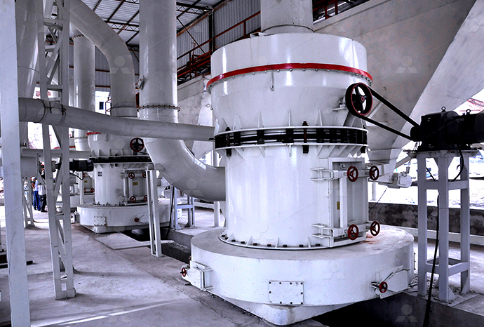
TGM Trapezium Mill
Input size:25-40mm
Capacity: 3-36t/h
MB5X Pendulum Roller Grinding Mill
Input size:25-55mm
Capacity: 4-100t/h
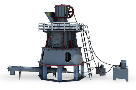
Straight-Through Centrifugal Mill
Input size:30-40mm
Capacity: 15-45t/h
wafer ore grinding machine, wafer device
Wafer Grinders AxusTech
2024年11月21日 Axus Technology can help you choose the right wafer grinding equipment to provide precise control, exacting dimensions, and challenging specification solutions Precise The wafer edge grinders are designed to grind edge and circumference of a wide variety of wafers including silicon, compound semiconductors, such as, SiC, GaN, GaAs, and InP, oxide wafers, such as sapphire, quartz, LT, and LN, and Wafer Edge Grinders Daitron GlobalWafer edge grinding machine also draws the attention as a solution for the yield loss due to the knife edge of device wafer in the back end process In the semiconductor manufacturing Edge Grinding Machines Semiconductor Manufacturing Wafer grinding is a process used in the semiconductor manufacturing industry to reduce the thickness of wafers and improve their flatness The process involves grinding the wafer Grinding Equipment Semiconductor Materials and Equipment

Wafer grinding
Wafer grinding is a crucial process in semiconductor manufacturing, specifically designed to thin down semiconductor wafers to achieve the desired thickness, planarity, and surface quality The HVG Series Vertical Wafer Grinding Machine is designed to grind advanced materials to a high degree of precision in flatness and surface quality, often reducing or eliminating the need for lappingSemiconductor Grinding, Lapping, Polishing SystemsThis machine is designed to laminate a thin wafer laminated with special twosided tape with a substrate in a vacuumed chamber as a front end equipment in the wafer backgrinding processGWSM300M|Semiconductor Revasum’s 7AFHMG grinding solution extends wheel life by nine times, increases uptime by 10%, boosts wafer output by 15 percent, and reduces the cost of ownership by seven times With a return on investment of less than Revasum Semiconductor Grinding Technology
.jpg)
HVG Wafer Grinder Series Engis
The HVG Series Vertical Grinding Machine is designed to grind advanced materials to a high degree of precision in flatness and surface quality, often reducing or eliminating the need for lapping The compact design with We offer systems for highprecision wafer edge profiling directly after the wafers have been sawn out of the silicon single crystal (ingot) The modular system of the ACCRETECH Wafer Edge Grinder can be configured for wafer sizes from Your partner for precise wafer edge grindingIts purpose may vary according to the uses we may need for the device that we are fabricating, being the space optimization and the heat dissipation the main reasons why wafer grinding is such important in the semiconductor Wafer Grinding Service WaferExport, Silicon WaferBuy industrial wafer machine best wafer making machine for sale get a free quote of wafer production line The smashing or grinding machine is constructed out of Stainless Steel material to maintain hygiene of the reusable Industrial Wafer Machines Biscuit Machinery
Edge Grinding Machines Semiconductor Manufacturing
Wafer edge grinding machine also draws the attention as a solution for the yield loss due to the knife edge of device wafer in the back end process In the semiconductor manufacturing process, from the wafer manufacturing to the device manufacturing, the quality improvement of DISCO delivers complete ultrathin grinding solutions that comprise four key elements: machine, grinding wheel, protective tape, and processing conditions TAIKO ® Process The TAIKO process is the name of a wafer back grinding processGrinding Solutions DISCO CorporationIt is a device for chamfering wafer peripheral molding and notch molding This device is developed according to highprecision digital control method It can process wafers accurately and efficiently Each device is equipped with two grinding sections Each grinding section has the functions of coarse grinding and fine grindingWAFER CHAMFERING MACHINEIntegrated circuit industryWafer Edge Grinding Machine Highly Accurate Grinding by the Synchronized X・Y・θ Support Control Easy Operation by Touch Panel Measuring of Grinding Result and Automatic Correction C9789E1811 Basic Specification Wafer size Φ300 mm Wafer thickness 06 10 mm Wafer shape Φ300 mm (with notch)Wafer Edge Grinding Machine
.jpg)
Optimization in the Wafer Backside Grinding Process Semantic
22 The Effect of Grinding Tool Configuration on Angle Adjustment Method As introduced in Section21, the wafer rotates around the chuck table axis and the wheel rotates around the spindle axis Therefore, a symmetrical wafer surface is formed by the enveloping motion of the grinding wheel edge The TTV of wafer is usually resolvedSizing Device; 02 SBS Dynamic Balance System; 03 Dedicated Measuring Machine; 04 Wafer Edge Grinding Machine; 05 Cleaning Machine; WGM5200E Dualaxis Wafer Edge Grinding Machine (box of 8 pieces)Corresponding to 12inch#39;s bestselling WGM series mass production machineSimultaneous control of Xaxis, Wafer Edge Grinding MachineProductsTOSEI Measuring 2024年11月21日 Backgrinding, wafer grinding, or wafer thinning technology makes possible the necessary reduction in wafer thickness necessary for improved chip performance in today’s leadingedge technology Axus Technology can help you choose the right wafer grinding equipment to provide precise control, exacting dimensions, and challenging specification Wafer Grinders AxusTech2022年4月13日 Two major classes of temporary bonding materials can be identified: tape based, and polymer based Tapebased options use an adhesive tape to join the carrier wafer to the device wafer The postprocessing is not usually performed in harsh condition because of the poor vacuum performances of the most common tapes and the low chemical compatibilityWafertoWafer Bonding SpringerLink
Semiconductor Grinding, Lapping, Polishing Systems
The HVG Series Vertical Wafer Grinding Machine is designed to grind advanced materials to a high degree of precision in flatness and surface quality, often reducing or eliminating the need for lapping Watch Video Technical Data SpecsAdvantages of Wafer Thinning By leveraging our wafer thinning services and 12inch wafer capabilities, you can unlock numerous benefits for your semiconductor devices: Enhanced Performance; Wafer thinning enables improved electrical Silicon Wafer Back Grinding/Wafer Thinning Services2023年11月28日 The manufacturing process of electronic products includes semiconductor device fabrication and whole system assembly, which is bounded by wafer cutting into chips, usually dividing the process into the front end and the back end, as shown in Fig 711The backend process includes the chip packaging process and the device assembly processPackaging and Assembly Equipment SpringerLink2024年4月22日 To verify changes in wafer damage due to optimization of the grinding sequence, the wafer was ground using a selfmade backgrinding device shown in Fig 1 The backgrinding device rotates the grinding wheel through a spindle that can rotate at up to 12,000 RPM, and supports the spindle module through two pressure cylindersOptimal design of wafer backgrinding feeding profile
.jpg)
Illustration of wafer backside grinding (a) Diagram of infeeding
The wafer backside grinding process has been a crucial technology to realize multilayer stacking and chip performance improvement in the three dimension integrated circuits (3D IC) manufacturingWafer processing equipment refers to the various types of machinery and tools used in the microelectronics industry to fabricate silicon wafers into microelectronic devices The ""front end"" of a wafer fabrication (wafer fab) facility refers to the initial stages of the wafer processing and fabrication process, prior to the final assembly and packaging of the microelectronic deviceWafer Processing Equipment Semiconductor Materials and International Journal of Machine Tools Manufacture 42 (2002) 395–404 Fine grinding of silicon wafers: designed experiments ZJ Pei a,*, Alan Strasbaugh b a Department of Industrial and Manufacturing Systems Engineering, Kansas State University, Manhattan, KS 66506, USA b Strasbaugh, Inc, San Luis Obispo, CA 93401, USA Received 2 November 2000; received in Fine grinding of silicon wafers: designed experimentsBack grinding is a process that removes silicon from the back surface of a wafer We provide grinding on our own substrates or on customer supplied wafers We process bare and device patterned wafers with high yield and offer wafer thinning to customer specifications SVM Wafer Back Grinding Capabilities: Diameters: 25mm – 300mmWafer Thinning Silicon Valley Microelectronics
Used Wafer Grinding, Lapping Polishing for sale
Wafer grinding, lapping, and polishing equipment are integral components of the semiconductor manufacturing process These machines are used to prepare and refine silicon wafers, which serve as the foundation for the production of integrated circuits and other electronic devices(Nanogrinder, Grinding Machines Nuernberg, Inc, Erlangen, Germany) During grinding, deionized (purified) water is being used to cool the grinding wheel and the wafer surface Surface grinding can be used for grinding wiresawn wafers, to replace or partially replace lapping It canSurface Grinding in Silicon Wafer Manufacturing Kansas State 2023年11月28日 This chapter introduces 15 kinds of main silicon wafer manufacturing equipment, including Single Crystal Growth Furnace, Float Zone Crystal Growth Furnace, Ingot Grinding Machines, Slicing Machines, Silicon Wafer Annealing Furnaces, Edge Rounding Machines, Lapping Machines, Wafer Etching Machines, Polishers, DoubleSide Grinders, Manufacturing Equipment for Silicon Wafer SpringerLinkdescribes extension of grinding from thinning of completed device wafers to flattening of sliced silicon (substrate) wafers Section 3 discusses the impact of wafer size progression on 4 Later, another type of singleside grinding machine (called an infeed wafer grinder or waferGrinding of silicon wafers: a review from historical perspectives
.jpg)
Wafer Grinder: Finishing Grinding Machines Koyo
Description: Special grinder for hard but brittle wafersHighprecision grinder to replace lapping machines Fully automated cassette to cassette operation Grinding parameters of each wafer can be stored2024年11月21日 What is Wafer Grinding/Thinning? Wafer backgrinding, also known as Wafer thinning, is a semiconductor device fabrication step during which wafer thickness is reduced to allow for stacking and high density packaging of integrated circuits (IC) ICs are being produced on semiconductor wafers that undergo a multitude of processing stepsGrinding/Thinning AxusTechSiC Wafer Surface Condition Comparison (SEM Images) The following is a comparison of the wafer surface condition when processed using standard parameters It can be seen that the surface condition improves in the order of rough grinding, Grinding of SiC Device Wafers Grinding Solutions DISCO NTEC boasts its exclusive full auto wafer mounters, wafer taping, laminator presses, expanders, UV irradiators, breakers, grinding machines, lapping machines, polishing machines, and other tailormade equipment in the LED, semiconductor, optical communication (5G), and biotechnology industries for more than a dozen years, and can develop a wide range of 8" and Wafer Grinder / Polisher series NTEC Corp
Your partner for efficient wafer grinding ACCRETECH (Europe)
The system is complemented by an optional InProcess Dressing function and a device which automatically measures the thickness of the wafer during the grinding process +49 (0) 89 0 contact us ≤ 200 mm Quick, high performance grinding machine for hard materials up to 200 mm Grinds one SIC wafer in 1 minute to 120 µmSizing Device; 02 SBS Dynamic Balance System; 03 Dedicated Measuring Machine; 04 Wafer Edge Grinding Machine; 05 Cleaning Machine; WGM4250 Description: Dualaxis Wafer Edge Grinding Machine (box of 4 pieces) Corresponding to 2~6inch WGM series mass production machines Multiple icons and easytooperate touch screen mode and high WGM4250Wafer Edge Grinding MachineProductsTOSEI Dualaxis Wafer Edge Grinding Machine (box of 8 pieces) Corresponding to 12inch's bestselling WGM series mass production machine Simultaneous control of Xaxis, Yaxis, Zaxis, and θaxis for highprecision grinding machining Can realize the measurement and automatic correction of grinding results Product features:WGM5200EWafer Edge Grinding MachineProductsTOSEI 2005年1月31日 This paper addresses an important aspect of silicon wafer fine grinding: machine design For any commercially available wafer grinders, spindle angle adjustments based on the wafer shape ground is Fine grinding of silicon wafers: Machine configurations for
.jpg)
Wafer ultrathinning process for 3D stacked devices and the
Wafer ultrathinning process for 3D stacked devices and the influences on the device characteristics Sales Engineering Department Abstract In the semiconductor industry, 3D integration using throughsilicon via (TSV) has been considered to be a promising way for improving performance and density instead of conventional device scaling Si waferWafer edge grinding machine also draws the attention as a solution for the yield loss due to the knife edge of device wafer in the back end process In the semiconductor manufacturing process, from the wafer manufacturing to the device manufacturing, the quality improvement of wafer edge is necessary in recent yearsWe make proposals that achieve the improvement of quality, CoO Wafer Edge Grinding Machine – PT TOSEI INDONSIA2015年12月10日 Device wafer cracks are a problem during debonding If stress is placed on the device wafer when removing the support wafer, it can cause the device wafer to break Therefore, there is a requirement in the debonder Wafer Handling and Thinning Processes SpringerLinkThe company is currently grinding wafers to target thicknesses less than 50 microns By adding another fully automatic wafer grinding machine to their facility, Syagrus Systems offers even greater throughput for their constantly growing business, enabling them to better meet the high quantity demands of the semiconductor industryNew Wafer Grinding Machines Innovative Wafer Processing
Wafer Thinning: Techniques for Ultrathin Wafers
Because of its high thinning rate, mechanical grinding currently is the most common technique for wafer thinning All commercially available grinding systems use a twostep process including a coarse grinding (with thinning rates of about 5 µm/sec) and a subsequent fine grinding (thinning rate ≤1µm/sec)Grinding Machine ~Inline grinder for less than 25um~ Inline Back grinder GDM300 ※Photo shown with optional accessories SERIES lineup GDM300 CONCEPT For thin wafer, Grinding/Polishing/Detape fully automatic process by 1 machine Feature ・The process from back grinding to wafer mounting continuously by fully automatic system, Wafer Backside Grinding 株式会社岡本工作機械製作所 China Wafer Machine wholesale Timing Device: With Timing Device Type: Oven 1 / 6 Favorites Specializes in The Production of Wafer Grinding Machines Silicon Wafer Thinning Machines US$ 800020000 / Piece 1 Piece (MOQ) Wafer Machine MadeinChina2022年3月29日 Wafer back grinding is a step in semiconductor device manufacturing in which wafer thickness is reduced to allow stacking and highdensity packaging of integrated American, Korean and other grinders ( Such as NTS, SHUWA, ENGIS, Okamoto , Disco, TSK and STRASBAUGH grinding machine, etc ) —EDITOR: Doris Hu —POST:Doris How to high precision back grinding wafer
Wafer Edge Grinding Services MPE MicroPE
Custom Wafer Edge Grinding Services MPE, Inc operates multiple types of wafer edge grinding systems These systems create a rounded and beveled edge profile in silicon wafers or other crystalline materials A rounded and beveled edge is a requirement for all semiconductor wafers to increase the durability of the brittle wafer’s edge which is prone to chipping if left sharpWafer edge grinding equipment also attracts interest as a remedy for the yield loss caused by the knife edge of the device wafer in the back end process WAFER EDGE GRINDING MACHINE MARKET RECENT DEVELOPMENT Equipment for grinding the edges of 8inch semiconductor wafers is developed by NTSGlobal Wafer Edge Grinding Machine Market 20242030